In digital circuit design, 10K resistor networks are among the most frequently used passive components. From microcontroller pull-up/pull-down and I²C bus level matching to ADC reference voltage division, they can be found in almost every functional module. You may have noticed that behind the seemingly simple '10K', three core parameters—pin configuration, rated power selection, and accuracy class—directly determine circuit stability, power consumption, and signal integrity. This manual is data-driven, systematically deconstructing the core technical parameters of 10K resistor networks to help you make precise decisions during the selection and layout stages.
1. Fundamentals and Common Types of 10K Resistor Networks

1.1 What is a 10K Resistor Network: Resistance Definition and Circuit Roles
A 10K resistor network refers to a device that integrates multiple resistors with a resistance value of 10,000Ω into a single package under a specific topology. Why has 10K become the 'default resistance' for digital circuits? The reason is that under a 5V logic level, a 10K pull-up consumes only 0.5mA of current. This ensures sufficient drive capability without causing excessive static power consumption—representing a long-proven engineering compromise between speed and power dissipation.
Compared to discrete resistors, the core advantages of resistor networks lie in their matching precision and space efficiency. Resistors within the same package are manufactured simultaneously using the same process, allowing relative tolerances to be controlled within ±0.1%, whereas the matching error of discrete resistors is typically above ±1%. Typical application scenarios include SDA/SCL pull-ups for I²C buses, pull-ups for MCU reset pins, ADC input voltage divider networks, and LED current-limiting arrays.
1.2 Mainstream Package Styles and Internal Topologies
The package style of a 10K resistor network directly determines its application scenarios. In an isolated network, each resistor is completely independent, making it suitable for applications with high signal isolation requirements; a bussed network connects one end of all resistors to a common terminal, ideal for pull-up/pull-down arrays; an isolated topology provides complete electrical isolation between channels, used in high-voltage or multi-ground systems.
| Package Type | Pin Count | Typical Topology | Application Scenarios |
|---|---|---|---|
| SIP | 4-14 | Bussed / Isolated | Through-Hole Prototyping |
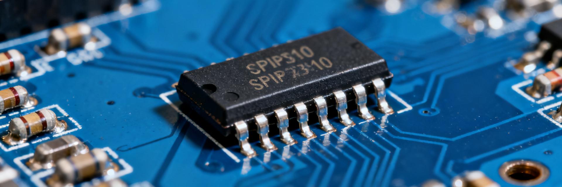
| SOP | 8-16 | Isolated | SMT Mass Production |
| QFN | 16-24 | High-Density Array | Portable Devices |
Identifying the common pin (Common Pin) is the first step of the layout. In a bussed network, the common pin is typically located at one end of the package (such as Pin 1) and must be connected to power or ground. Correctly identifying the common pin prevents signal crosstalk and current loop errors.
2. Deep Dive into Pin Configuration: From Pin Definition to Layout Keypoints
2.1 Pin Function Definitions and Typical Wiring Schemes
Each pin of a 10K resistor network plays a distinct role in the circuit. Taking a pull-up network as an example: the common terminal is connected to VCC, and each output pin is connected to the MCU's GPIO or bus signal lines. Conversely, in a pull-down network, the common terminal is grounded, and each pin is connected to a signal line. In multi-channel networks, pin multiplexing requires special attention to signal crosstalk: parasitic capacitance between adjacent channels can degrade high-speed signal edges, so it is recommended to interleave sensitive signal channels during layout.
2.2 Impact of Pin Configuration on Circuit Performance
The impact of pin parasitic inductance and capacitance on high-speed signal integrity cannot be ignored. For example, in an I²C bus, a standard 10K pull-up resistor paired with a typical 100pF bus capacitance yields a rise time of approximately 2.2μs—which is feasible for the 400kHz Fast-mode but requires reducing the resistance for high-speed modes above 1MHz. Pin spacing and creepage distance are especially critical in high-voltage scenarios: according to the IEC 60950 standard, the minimum creepage distance under a 250V working voltage should be no less than 1.5mm.
PCB layout and routing recommendations: shorten lead lengths, reduce the number of vias, and optimize return paths. For 10K pull-up networks, it is recommended to place the network device close to the signal source rather than the receiver to minimize reflections.
2.3 Comprehensive Analysis of Power Parameters: Rated Power, Derating, and Thermal Design
Common rated power levels include 0.125W, 0.25W, 0.5W, and 1W. The selection is based on the derating curve representing the relationship between actual power dissipation and ambient temperature. For instance, a 0.25W network at an ambient temperature of 70°C may see its allowable power dissipation drop to 60% of its rated value—namely, 0.15W. The single-channel power dissipation formula is P = V²/R: with a 5V pull-up, each 10K resistor consumes 2.5mW, and the total power dissipation for 8 channels operating simultaneously is 20mW, which is far below the derating limit.
Failure modes under power overload include resistance drift, open circuits, and thermal breakdown. Thermal dissipation measures include increasing copper foil area, placing thermal vias, and optimizing the network array layout. In scenarios where multiple channels operate simultaneously, total power dissipation and temperature rise assessments should be conducted as pre-selection steps.
3. Precision Parameters and Matching Characteristics: Tolerance, TCR, and Long-Term Stability
3.1 Accuracy Classes and Tolerance Selection
Common tolerance classes are ±1%, ±2%, and ±5%. The ±5% tolerance is suitable for pull-up/pull-down scenarios where accuracy requirements are low and cost is minimized; ±1% is used for applications requiring precise ratios, such as ADC voltage division; and ±0.1% is reserved for precision measurement instruments. Accuracy allocation in voltage divider circuits requires calculating the total system error: if both resistors have a ±1% tolerance, the worst-case divider ratio error can reach ±2%.
3.2 Temperature Coefficient of Resistance and Long-Term Stability
The Temperature Coefficient of Resistance (TCR) is defined as the relative change in resistance caused by a unit change in temperature, with typical values of ±100ppm/°C, ±50ppm/°C, and ±25ppm/°C. For a 10K resistor with ±100ppm/°C, as the temperature rises from 25°C to 85°C, the resistance shifts by 600Ω (0.6%). In full-temperature-range error budgeting, the contribution of TCR cannot be ignored.
Regarding long-term stability, load life and shelf life are two core indicators. A high-quality 10K resistor network operating at rated power for 1,000 hours typically exhibits a resistance drift of less than 0.5%. For precision applications, it is recommended to prioritize products with TCR ≤ ±50ppm/°C and those that have undergone burn-in screening.
4. Selection and Substitution Guide: Parameter Trade-Offs and Supply Chain Considerations
4.1 Key Parameter Priority and Selection Flowchart
During selection, parameter priority must be determined based on the application scenario. For I²C pull-ups, pin configuration and power are prioritized; for ADC voltage division, precision and TCR take precedence. The selection checklist should include: resistance, power, tolerance, TCR, package style, and pin count. Common selection pitfalls include: ignoring the derating curve, which leads to insufficient power at high temperatures, and confusing absolute tolerance with relative tolerance, leading to excessive matching errors.
4.2 Substitution and Compatibility Evaluation
Criteria for pin-compatible substitution include: topology, common terminal position, and pin pitch. For electrically compatible substitution, the power margin, accuracy class, and TCR matching must be evaluated. Supply chain multi-sourcing strategy recommendation: avoid single-source risks by prioritizing standard package products with second-source options. For 10K resistor networks, SOP-16 and QFN-24 packages typically offer excellent multi-source availability.
Key Takeaways
- The 10K resistor network is the default resistance choice for digital circuits, with its core advantages being matching precision and space efficiency. It is suitable for pull-up, pull-down, voltage-dividing, and current-limiting scenarios.
- Pin configurations directly impact signal integrity and layout efficiency; key design points include identifying the common terminal in bussed networks and controlling pin parasitic parameters.
- Power parameters must be evaluated alongside derating curves; a 0.25W network's usable power drops to 0.15W at 70°C, and the total power dissipation of multiple channels should be calculated in advance.
- Precision and TCR determine the system's measurement error; a ±1% tolerance combined with a ±50ppm/°C TCR meets the requirements of most precision applications.
- Selection should follow a parameter-prioritized workflow, and when substituting, both pin compatibility and electrical compatibility must be evaluated simultaneously to avoid single-source supply chain risks.
Frequently Asked Questions (FAQ)
How does the accuracy class of a 10K resistor network affect ADC sampling errors?
In ADC voltage divider circuits, resistor tolerance directly translates into divider ratio error. If both 10K resistors have a ±1% tolerance, the worst-case divider ratio error is ±2%, corresponding to an error of approximately 82 LSB in a 12-bit ADC. If a ±0.1% matched resistor network is selected, the error can be reduced to within ±0.2%, which is about 8 LSB. Therefore, high-precision matched networks should be prioritized for precision sampling.
How to select the rated power of a 10K resistor network based on ambient temperature?
It is necessary to refer to the device's power derating curve. Typically, a 0.25W network has a derating factor of approximately 60% at an ambient temperature of 70°C, reducing the allowable power dissipation to 0.15W. When calculating actual power consumption, use the formula P=V²/R: with a 5V pull-up, each channel consumes 2.5mW, resulting in a total power consumption of 20mW for 8 channels, which is far below the derating limit. However, if used in power driving scenarios, 80% of the derated power should be used as the design margin.
How does the pin configuration of a 10K resistor network affect the signal integrity of the I²C bus?
The pin parasitic capacitance and the bus capacitance together determine the rise time. A standard 100pF bus capacitance paired with a 10K pull-up results in a rise time of approximately 2.2μs, which is suitable for the 400kHz Fast-mode. If the bus capacitance increases to 200pF, the rise time doubles to 4.4μs, which may cause timing violations in high-speed modes. In this case, the pull-up resistance should be decreased, or a resistor network with low-capacitance packaging should be selected.
Which parameters must be strictly matched when replacing a 10K resistor network?
The pin topology, common terminal position, and pin pitch must be strictly matched to ensure physical compatibility. Electrically, the power margin must not be reduced, and the accuracy class and TCR should be at least equivalent. If the original design uses a ±1%/±100ppm/°C product, the replacement should not fall below this standard. It is recommended to perform in-circuit testing after replacement to verify signal integrity and temperature stability.